-
Korean Equities/Company Deep Dives
Samsung vs. SK Hynix: Two Very Different Bets on AI Memory's Next Bottleneck
2026. 8. 10.
Table
반응형At FMS 2026, the world's largest memory and storage industry event, Samsung Electronics and SK Hynix unveiled two fundamentally different answers to the same problem: AI accelerators are increasingly bottlenecked not by compute power, but by how fast memory can feed them data. SK Hynix, partnering with SanDisk, is betting on capacity. Samsung is betting on proximity. Understanding both approaches — and why combining them might be the more interesting story — matters for anyone tracking Korea's two memory giants.
Table of Contents
- From HBM to the Next Memory Bottleneck
- SK Hynix and SanDisk's Answer: HBF
- Samsung's Answer: zHBM
- A Kitchen Analogy for the Two Approaches
- Could the Two Approaches Be Combined?
- Open Questions: Camps, Heat, and Yield
- Timeline: Who's Further Along
- Bottom Line
From HBM to the Next Memory Bottleneck
Modern AI systems run on a CPU-GPU-HBM-NAND memory hierarchy, each layer solving a speed or capacity limitation of the one before it. GPUs handle massive parallel computation, DRAM provides working memory, and High Bandwidth Memory (HBM) sits physically adjacent to the GPU to feed it data quickly. But HBM isn't suited for holding large volumes of data long-term — that role falls to NAND flash storage, which is far cheaper and higher-capacity, but also considerably slower and physically farther from the compute engine.
This gap matters more than it might seem: GPUs reportedly spend only 20-30% of their time actually computing during AI workloads, with the remainder consumed by waiting on data — and NAND's distance and latency is one of the largest contributors to that wasted time. Solving this bottleneck is exactly what Samsung and SK Hynix are now racing to do, using two distinctly different strategies.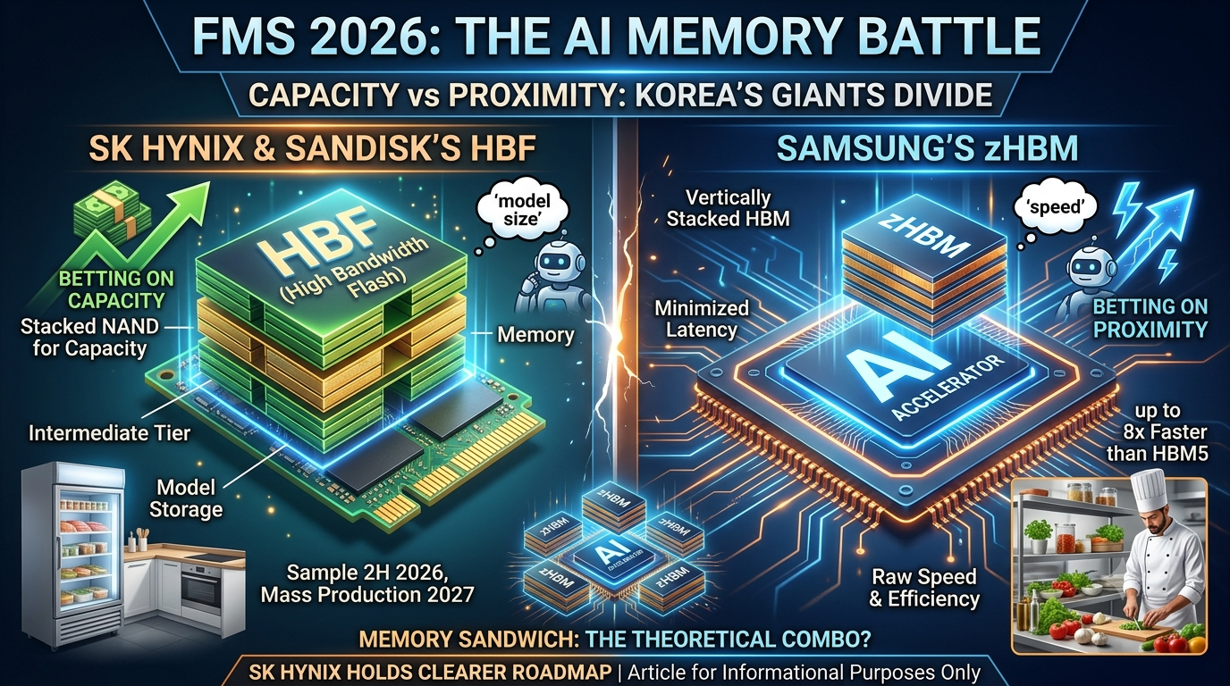 반응형
반응형SK Hynix and SanDisk's Answer: HBF
SK Hynix, in partnership with SanDisk (with Google also involved), is developing High Bandwidth Flash (HBF) — applying HBM's vertical stacking technique to NAND flash instead of DRAM. The goal isn't to replace NAND or HBM, but to insert a new intermediate tier between them: a large, relatively affordable buffer that sits closer to the compute engine than traditional SSD storage, positioned for AI inference workloads that need to hold large models cost-effectively. SK Hynix's HBM stacking expertise gives it a natural advantage in applying similar techniques to flash. The company has stated plans to release HBF samples in the second half of 2026, targeting mass production within 2027.
Samsung's Answer: zHBM
Samsung's answer, also unveiled at FMS 2026, is called zHBM — and rather than changing HBM's underlying material, it changes HBM's physical position. Traditional HBM sits beside the AI accelerator; zHBM stacks vertically on top of it instead, shortening the physical distance data needs to travel. Samsung claims zHBM could be up to 8 times faster than upcoming HBM5, with roughly 3 times better performance per watt of power. Unlike HBF's focus on capacity, zHBM targets raw speed and efficiency.
A Kitchen Analogy for the Two Approaches
Think of an AI accelerator as a chef, where cooking speed depends on how quickly ingredients reach the countertop. HBM is like keeping ingredients within arm's reach on the counter — fast to grab, but limited space. SSD is like a large basement storage room — plenty of capacity and cheap to maintain, but it takes real time to retrieve anything. HBF is like installing a commercial-grade refrigerator right next to the counter — no trip to the basement required, and it holds a meaningful amount of ingredients, though still somewhat slower than reaching directly to the counter. Samsung's zHBM, by contrast, puts the ingredients on a shelf directly in front of the chef rather than beside them — potentially faster still, and requiring less physical effort to access.
Could the Two Approaches Be Combined?
Since HBF optimizes for capacity and cost while zHBM optimizes for speed and efficiency, an intriguing possibility is combining both: the accelerator surrounded by memory above, beside, and below in a three-dimensional "memory sandwich." In this hypothetical structure, zHBM on top would hold actively used data, HBF in the middle would store the full model and large-scale NAND capacity, and SSD at the bottom would hold rarely accessed cold data — potentially eliminating both the "high capacity, but slow" and "fast, but limited" dilemmas simultaneously, since the full model would live in HBF with only the actively needed portion elevated to zHBM.
Open Questions: Camps, Heat, and Yield
Several practical hurdles remain before any combined approach could materialize. The most immediate is competitive alignment: HBF is a joint SK Hynix-SanDisk effort, while zHBM is Samsung's proprietary technology — meaning combining them would require unusual cross-camp cooperation. Samsung has also unveiled zNAND-O, its own high-performance NAND technology shown alongside zHBM at FMS 2026, suggesting Samsung may prefer pairing zHBM with its own NAND rather than integrating with a competitor's HBF.
Thermal management is a second major challenge — stacking memory directly on top of an already hot compute chip creates significant heat dissipation problems, which would only compound if flash storage were layered around it as well. Manufacturing yield is a third concern: in a tightly integrated stacked structure, a single component failure could render the entire assembly unusable, potentially resulting in very low yields.Timeline: Who's Further Along
On execution timelines, SK Hynix currently appears further along: Samsung's zHBM and zNAND-O remain concept demonstrations with no confirmed commercialization date, while SK Hynix has published a concrete roadmap — samples in the second half of 2026, mass production targeted within 2027.
Bottom Line
At FMS 2026, SK Hynix and SanDisk revealed HBF, targeting AI memory capacity and cost efficiency through stacked NAND, while Samsung unveiled zHBM, targeting speed and power efficiency by repositioning HBM directly atop the accelerator. The two approaches solve different halves of the same bottleneck, and while combining them into a unified 3D memory structure remains theoretical given cross-camp competition, thermal, and yield challenges, SK Hynix currently holds a clearer execution timeline toward commercialization.
This article is for informational purposes only and does not constitute investment, tax, or legal advice. Readers should consult a licensed professional before making investment decisions.
반응형'Korean Equities > Company Deep Dives' 카테고리의 다른 글
Korean Stock & Equity Research
Data-driven analysis of Korean listed companies, combining financial fundamentals with supply chain and operations insights. Not investment advice.